Explore our wide range of high-quality products and solutions tailored to meet your needs.

Design/Engineering process
PCB Layout & Design
Design/Engineering process
PCB Layout & Design is the process of planning and drawing the physical arrangement of an electronic circuit on a printed circuit board (PCB).
Two Main Parts
1. PCB Design (Schematic Design)
- Create the circuit diagram
- Define:
- Components (resistors, ICs, etc.)
- Electrical connections (nets)
2. PCB Layout
- Arrange components on the board
- Route tracks (copper paths) to connect them
- Decide board shape and layers
Steps in PCB Layout & Design
1. Schematic Creation
- Draw circuit using tools like
Altium Designer or KiCad
2. Netlist Generation
- Software generates list of all connections
3. Component Placement
- Components arranged logically:
- ICs first
- Then supporting components
4. Routing (Track Design)
- Copper traces drawn to connect components
- Can be:
- Manual routing
- Auto-routing
5. Layer Stack Design
- Decide:
- Single-layer / double-layer / multi-layer
6. Design Rule Check (DRC)
- Ensures:
- No short circuits
- Proper spacing
- Manufacturability
7. Output Files Generation
- Files like:
- Gerber files (used for fabrication)
Objectives of PCB Design
- Ensure correct electrical connections
- Minimize noise and interference
- Optimize space and cost
- Improve performance and reliability

Our Products
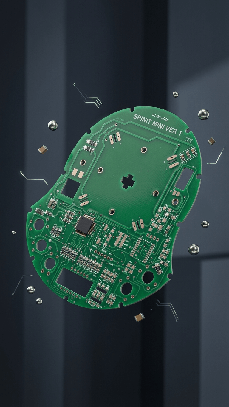
PTH Double Sided PCB
Plated Through Hole (PTH) double-sided PCBs offering higher circuit density, strong mechanical bonding, and enhanced reliability.
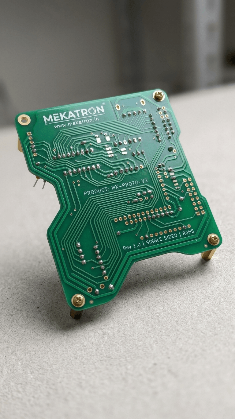
Single Sided PCB
Reliable single-layer printed circuit boards ideal for simple electronic applications and power supplies.
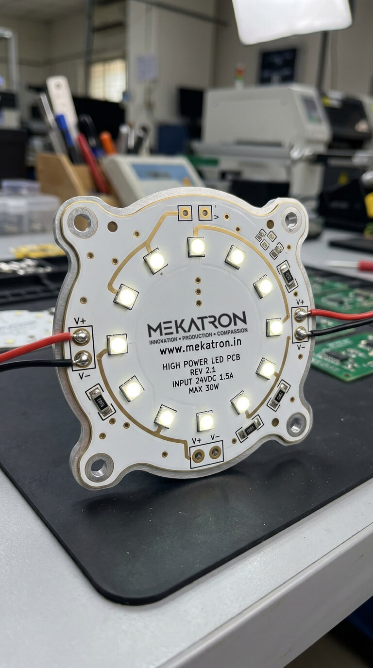
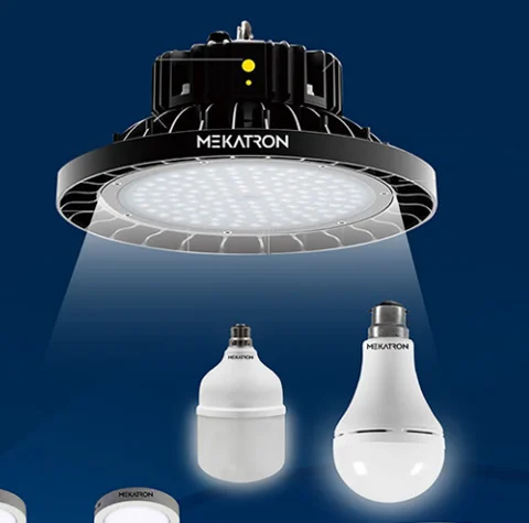
Aluminum Metal Core PCB
Metal Core PCBs specially designed for LED applications, ensuring excellent heat dissipation and longer product life.